Vacancies at iCALL Psychosocial Helpline, TISS
Vacancies at iCALL Psychosocial Helpline, Tata Institute of Social Sciences (TISS). Counselor Post in iCALL Psychosocial Helpline TISS via Direct …
Vacancies at iCALL Psychosocial Helpline, Tata Institute of Social Sciences (TISS). Counselor Post in iCALL Psychosocial Helpline TISS via Direct …
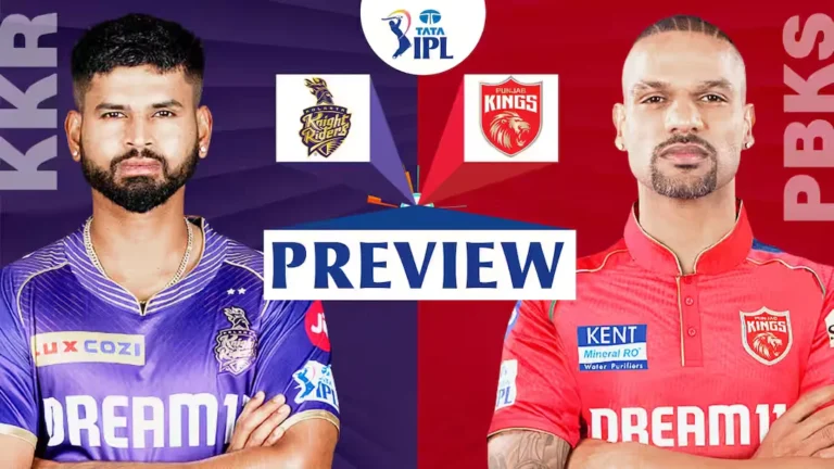
KKR vs PBKS | 42nd Match | Indian Premier League 2024. Kolkata Knight Riders vs Punjab Kings, 42nd Match – …

SRH vs RCB | 41st Match | Indian Premier League 2024. Sunrisers Hyderabad vs Royal Challengers Bangalore, 41st Match – …

DC vs GT | 40th Match | Indian Premier League 2024. Delhi Capitals vs Gujarat Titans, 40th Match – Live …
KAV Barpeta Recruitment 2024 – 19 Assistant Professor & Deputy Registrar Vacancy. KAV Barpeta Recruitment 2024: Teaching & Non Teaching …
Jawahar Navodaya Vidyalaya Recruitment 2024: Advertisement-Contractual appointment of TGT,PGT for session 2024-25. Jawahar Navodaya Vidyalaya Recruitment 2024: TGT,PGT Jawahar Navodaya …

CSK vs LSG |39th Match | Indian Premier League 2024. Chennai Super Kings vs Lucknow Super Giants, 39th Match – …

RR vs MI | 38th Match | Indian Premier League 2024. Rajasthan Royals vs Mumbai Indians, 38th Match – Live …
PBKS vs GT | 37th Match | Indian Premier League 2024. Punjab Kings vs Gujarat Titans, 37th Match – Live …
TISS Mumbai Recruitment 2024: Advertisement for the post of Social Worker at Prayas, TISS Mumbai. TISS Mumbai Recruitment 2024: Social …
SSA Dispur Recruitment 2024 – Apply for Teacher Vacancy. Applications are invited for recruitment of various teaching positions or career …
UGC-NET June 2024: Online Application Form. Opening of the online portal for submission of Online Application Form for UGC-NET June …

KKR vs RCB | 36th Match | Indian Premier League 2024. Kolkata Knight Riders vs Royal Challengers Bengaluru, 36th Match …

DC vs SRH | 35th Match | Indian Premier League 2024. Delhi Capitals vs Sunrisers Hyderabad, 35th Match – Live …
Indian Institute of Technology Dharwad Ph.D Admission 2024. Ph.D Admission Notification 2024-25. IIT Dharwad Admissions 2024: Eligibility, Dates, Application fees. …